


Nano-imprint
Surface microfabrication technology characterized by nano-sized resolutions
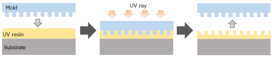
Nano-imprint technology is a microfabrication technology used for transferring nano-ordered patterns, developed based on embossing (concavity and convexity, and embossing treatment) technology.
There are 4 processes: application, press, transfer and demolding. Due to its simplicity, potential for mass production at low cost and relatively easy manipulation, this device is expected to become a highly promising microfabrication technology. Meanwhile, it is necessary to finely tune the device, processes, materials, etc., in order to improve the repeatability of high-precision products.
The advantage of UV imprint is its transfer time which is shorter than that of thermal imprint if the UV rays penetrate the mold.
Efforts are being made for practical application in a variety of fields such as semi-conductor devices, biotechnology, optical materials, etc.
Description of the video
- The process for applying resin to a plate and transfer it to a film is as described below.
For details, please contact us.![]()
- Related links
-
Technology application product
Application examples